|
Mario Lanza and co‐workers review the main challenges and potential solutions towards the fabrication of field effect transistors with 2D semiconducting channels. The scalability and compatibility of these materials with the requirements imposed by the semiconductor industry are discussed, and some recommendations are proposed. 
0 Comments
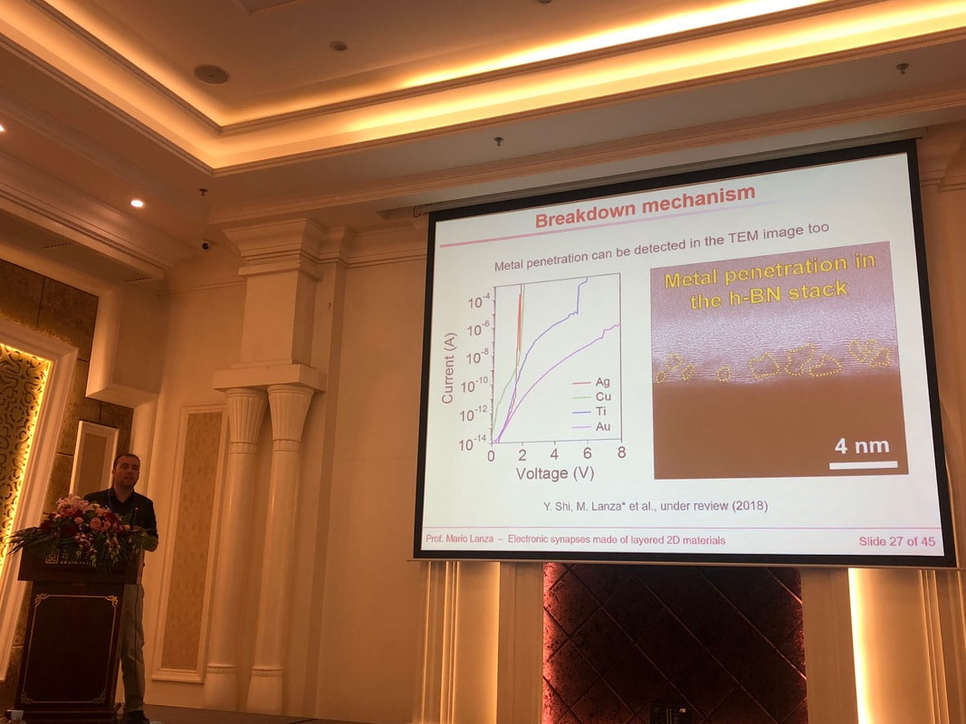
Engineering Field Effect Transistors with 2D Semiconducting Channels: Status and Prospects9/24/2019 Abstract The continuous miniaturization of field effect transistors (FETs) dictated by Moore's law has enabled continuous enhancement of their performance during the last four decades, allowing the fabrication of more powerful electronic products (e.g., computers and phones). However, as the size of FETs currently approaches interatomic distances, a general performance stagnation is expected, and new strategies to continue the performance enhancement trend are being thoroughly investigated. Among them, the use of 2D semiconducting materials as channels in FETs has raised a lot of interest in both academia and industry. However, after 15 years of intense research on 2D materials, there remain important limitations preventing their integration in solid‐state microelectronic devices. In this work, the main methods developed to fabricate FETs with 2D semiconducting channels are presented, and their scalability and compatibility with the requirements imposed by the semiconductor industry are discussed. The key factors that determine the performance of FETs with 2D semiconducting channels are carefully analyzed, and some recommendations to engineer them are proposed. This report presents a pathway for the integration of 2D semiconducting materials in FETs, and therefore, it may become a useful guide for materials scientists and engineers working in this field.  Chemical vapor deposition of hexagonal boron nitride on metal-coated wafers and transfer-free fabrication of resistive switching devicesAbstract Due to their outstanding electronic and physical properties, two-dimensional (2D) materials have attracted much interest for the fabrication of solid-state microelectronic devices. Among all methods to synthesize 2D materials, chemical vapor deposition (CVD) is the most attractive in the field of solid-state microelectronics because it can produce high quality 2D material in a scalable manner. However, the high temperatures (>900 °C) required during the CVD growth of the 2D materials impede their direct synthesis on metal-coated wafers due to prohibitive metal diffusion and de-wetting. This makes necessary carrying out the 2D materials CVD growth independently on metallic foils, and transfer them on the wafers using polymer scaffolds. However, this process is slower, more expensive, and can lead to abundant contamination and cracks in the 2D material. Here we present a facile method to allow the direct growth of multilayer hexagonal boron nitride (h-BN) on Ni-coated Si wafers, which consists on placing a protective cover 30 μm above the Ni surface. The resulting h-BN stacks have been used to fabricate Au/Ti/h-BN/Ni memristors with low cycle-to-cycle variability. This work contributes to the integration of 2D materials in solid-state micro- and nano-electronic technologies.  Congratulations to Prof. Mario Lanza for being selected as distinguished lecturer of EDS...3/1/2019 Recently, Professor Mario Lanza of the Institute of Functional Nano and Soft Materials of Soochow University was elected as Distinguished Lecturer (EDS Distinguished Lecturer) by the Institute of Electrical and Electronics Engineers (IEEE). Professor Lanza is selected mainly based on his outstanding contribution to the field of two-dimensional materials and electronic devices. It is reported that including Professor Lanza, only four scientists in mainland China have won this honor. The other three are: Professor Huang Ru from Peking University, Academician Liu Ming from the Chinese Academy of Sciences, and Ren Tianling from Tsinghua University. 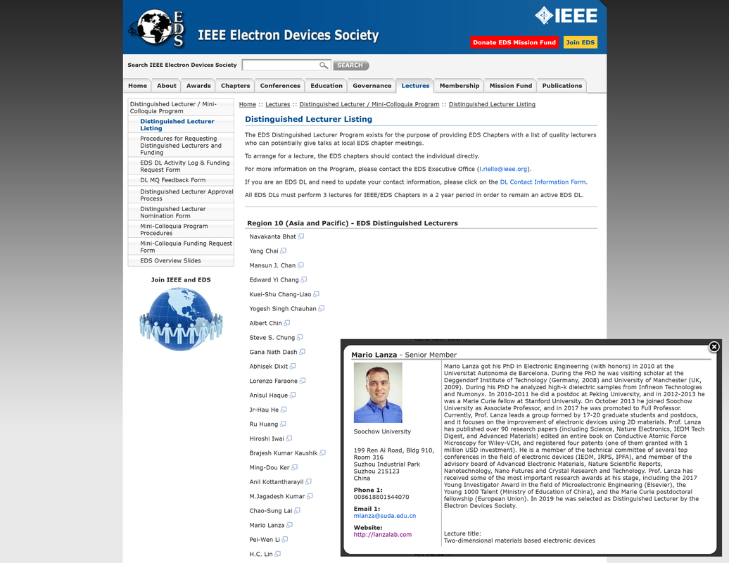  GTIIT is the first Chinese-foreign institute with independent legal person qualification to introduce excellent higher education resources from Israel in China. Collaborated by the Technion and STU, GTIIT is devoted to develop engineers and technological talents with innovation, global insight, and humanistic quality, with an aim to become a world-recognized high-level research-based institute in education, scientific research, and innovation. The Technion is a world-leading institute of higher education with three Nobel laureates and remains top 50 in global research-based university rankings. Since it was established in 1912, the Technion has been committed to the development of new technology and universally acknowledged as one of the world-top start-up ecosystems and an incubator for future successful entrepreneurs. STU has been sticking to an international and elaborate way of schooling, which has won close attention and great recognition from the educational circles at home and abroad. STU has been in the Times Higher Education World University Rankings for two years. From 2016-2017, it ranks No. 22 among the universities from Chinese Mainland on the list. Meeting with Prof. Moshe Eizenberg...That was a very nice meeting with him. There were a lot of fun during the lunch with him, especially, his early finding of "Carbon Monolayer", which may be the first grown graphene on the earth...
 The 2018 International workshop on future computing (IWOFC): memristive devices and systems is the 2nd in series providing an international forum for the discussion of recent advances and future prospects in future computing systems. The workshop will be held on December 17-18, 2018 at Hilton Shenzhen Shekou Nanhai, Shenzhen, China. The scopes of the workshop include theory, materials, devices, circuits, systems and other related research of future computing technology. The technological challenges and development trend of high intelligent and low power computing system will be discussed. Approximately over 200 workshop participants are expected to attend. Selected papers are scheduled to be published in the Science China Information Sciences. General Chair  Ru Huang, Peking Universiry General Co-Chair
Technical Program Committee Chair  Yuchao Yang, Peking University Venue
Best Global Universities for Materials Science, Soochow University (19th), by U.S. News.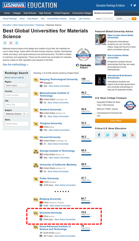 Best Chinese Universities for Nanoscience & Nanotechnology, Soochow University (5th), by Shanghai Ranking.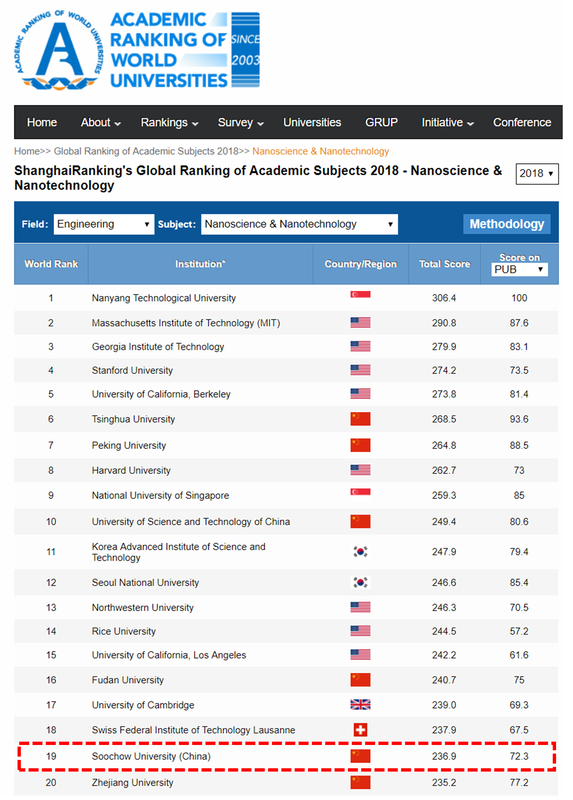 Statistical method for 2D material synthesis Photo of Prof. Cher Ming Tan Scheduled talk time: 29th of November, Room 308, Building 910.
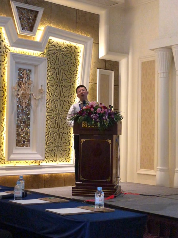
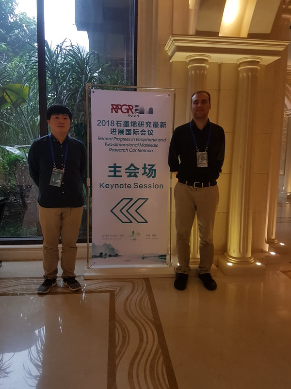
Abstract: 2D material possess interesting physical properties, and synthesis of 2D materials are one of the key material research topics. However, for the industrial synthesis of these 2D material, optimization of the synthesis through the identification of the key process parameters (also known as factors) must be identified. One-factor-at-a-time (OFAT) experimentation is the most common method to identify the key factors, in which only one factor or variable is varied at a time while keeping others fixed, but it suffers several limitations as will be discussed in this talk. The technique of Design-of-Experiments (DoE) is a Statistical wonder which enables efficient design of any process with respect to rational choice of key parameters. In this talk, the applications of DoE to Graphene growth or synthesis process as performed by my team will be presented. In this talk, I will highlight the prevalence of DoE technique in industrial processes and importance of DoE technique, and I will enunciate the need for DoE from the materials’ science point of view. Application of various concepts such as Attribute Response Design, Full Factorial DoE, and Filtered DoE approach to the novel Graphene Synthesis method will be discussed and explained briefly. This Filtered DoE is a modified DoE method developed by my team. Biography: Dr. Tan is a Singaporean, and he received his Ph.D in Electrical Engineering from the University of Toronto in 1992. He has 10 years of working experiences in reliability in electronic industry before joining Nanyang Technological University (NTU), Singapore as faculty member in 1996 till 2014. He joined Chang Gung University, Taiwan and set up a research Center on Reliability Sciences and Technologies in Taiwan and acts as Center Director. He is Professor in Electronic Department of Chang Gung University, Honorary Chair Professor in Ming Chi University of Technology, Taiwan, Adjunct Professor in the College of Medicine, and Researcher in the Chang Gung Memorial Hospital, Linkou. He has published 300+ International Journal and Conference papers, and giving 10+ keynote talks and 50+ invited talks in International Conferences and several tutorials in International Conferences. He holds 14 patents and 1 copyright on reliability software. He has written 4 books and 3 book chapters in the field of reliability. He is an Editor of Scientific Report, Nature Publishing Group, an Editor of IEEE TDMR, Series Editor of SpringerBrief in Reliability, and Associate editor of Microelectronic Reliability. He is a member of the advisory panel of Elsevier Publishing Group. He is a past chair of IEEE Singapore Section in 2006, senior member of IEEE and ASQ, Distinguish Lecturer of IEEE Electronic Device Society on reliability, Founding Chair and current Chair of IEEE Nanotechnology Chapter - Singapore Section, Fellow of Institute of Engineers, Singapore, and Fellow of Singapore Quality Institute. He is the Founding Chair of IEEE International Conference on Nanoelectronics, General Chair of ANQ Congress 2014. He is a recipient of IEEE Region 10 Outstanding Volunteer Award in 2011. He was Guest Editor of International J. of Nanotechnology, Nano-research letter and Microelectronic Reliability. He is in the reviewer board of several International Journals such as Thin Solid Film, Microelectronic Reliability, various IEEE Transactions, Reliability Engineering and System Safety etc. He is the first individual recipient of Ishikawa-Kano Quality Award in Singapore in 2014. He is active in providing consultation to multi-national corporations on reliability. His research interests include reliability and failure physics modeling of electronic components and systems, finite element modeling of materials degradation, statistical modeling of engineering systems, nano-materials and devices reliability, and prognosis & health management of engineering system. For more detail, please visit www.chermingtan.com On Oct. 22nd – 25th, Prof. Mario Lanza and I participated in the 10th annual Recent Progress in Graphene and Two-dimentional Materials Research Conference (RPGP 2018) in Guilin, China. In the conference, Prof. Mario Lanza was invited to give an invited talk on “Building the hardware of future artificial intelligence systems: two-dimentional materials based electronic synapses”. It’s a great experience to take part in the conference and we got the opportunity to interact with the top experts in the field.
Recommended Methods to Study Resistive Switching Devices Posted by Xu Jing Abstract Resistive switching (RS) is an interesting property shown by some materials systems that, especially during the last decade, has gained a lot of interest for the fabrication of electronic devices, with electronic nonvolatile memories being those that have received the most attention. The presence and quality of the RS phenomenon in a materials system can be studied using different prototype cells, performing different experiments, displaying different figures of merit, and developing different computational analyses. Therefore, the real usefulness and impact of the findings presented in each study for the RS technology will be also different. This manuscript describes the most recommendable methodologies for the fabrication, characterization, and simulation of RS devices, as well as the proper methods to display the data obtained. The idea is to help the scientific community to evaluate the real usefulness and impact of an RS study for the development of RS technology. 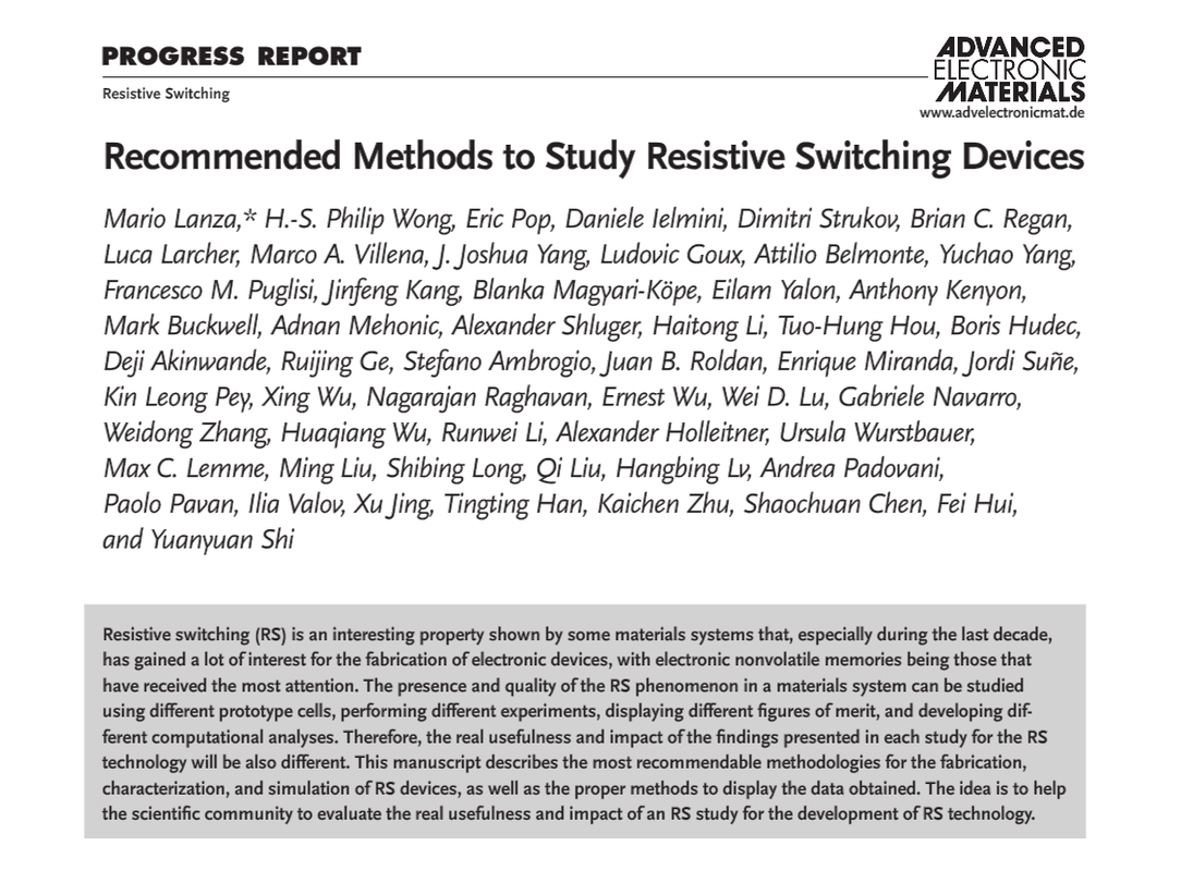 |
Xu JingPhD candidate, History
May 2020
Sorts
All
|


 RSS Feed
